| Platform | Process Node | Cryogenic Rating | Notable Strength | |----------|--------------|------------------|------------------| | (Quanta Labs) | 3 nm GAA | 10 mK – 300 K | Integrated SFQ + ultra‑low noise | | IBM Q‑Chip‑X | 5 nm FinFET | 4 K – 300 K | Mature fab, strong EDA flow | | Intel Xe‑Quantum | 7 nm | 4 K – 300 K | 3‑D integration with silicon‑spin qubits | | TSMC Q‑Lite | 3 nm (N5) | 4 K – 300 K | High‑volume fab, but no built‑in cryo‑IO |
| Parameter | Value (typical) | |-----------|-----------------| | | 3 nm Gate‑All‑Around (GAA) FinFET | | Substrate | High‑purity silicon‑on‑insulator (SOI, 100 nm buried oxide) | | Gate dielectric | 0.7 nm high‑κ (HfSiON) | | Operating temperature range | 10 mK – 300 K | | Cryogenic I/O | Integrated Single‑Flux‑Quantum (SFQ) drivers + 50 Ω differential pairs | | On‑chip memory | 256 Mb Embedded DRAM (eDRAM) optimized for 4 K operation | | Power density | ≤ 8 µW mm⁻² at 10 mK | | Noise floor | 6 µV RMS (1 Hz‑10 GHz) at 10 mK | | Packaging | Flip‑chip BGA with superconducting Nb interposers (thermal expansion‑matched) | | Yield | 99.9999 % (≥ 10 k die per wafer) |
| Timeline | Milestone | Impact | |----------|-----------|--------| | | Release of JUQ‑716‑H (high‑density variant, 2 nm gate length) | Enables 8 k‑qubit control on a single die | | 2027 | Standardization : IEEE 802.3bt‑Q (Cryogenic Ethernet) built on JUQ‑716 I/O | Inter‑node quantum networking becomes plug‑and‑play | | 2028 | Full‑stack “Quantum‑Ready” SoC : 1 TB/s bandwidth, 10⁶‑qubit support | Paves the way for fault‑tolerant quantum computers in the cloud |
| Platform | Process Node | Cryogenic Rating | Notable Strength | |----------|--------------|------------------|------------------| | (Quanta Labs) | 3 nm GAA | 10 mK – 300 K | Integrated SFQ + ultra‑low noise | | IBM Q‑Chip‑X | 5 nm FinFET | 4 K – 300 K | Mature fab, strong EDA flow | | Intel Xe‑Quantum | 7 nm | 4 K – 300 K | 3‑D integration with silicon‑spin qubits | | TSMC Q‑Lite | 3 nm (N5) | 4 K – 300 K | High‑volume fab, but no built‑in cryo‑IO |
| Parameter | Value (typical) | |-----------|-----------------| | | 3 nm Gate‑All‑Around (GAA) FinFET | | Substrate | High‑purity silicon‑on‑insulator (SOI, 100 nm buried oxide) | | Gate dielectric | 0.7 nm high‑κ (HfSiON) | | Operating temperature range | 10 mK – 300 K | | Cryogenic I/O | Integrated Single‑Flux‑Quantum (SFQ) drivers + 50 Ω differential pairs | | On‑chip memory | 256 Mb Embedded DRAM (eDRAM) optimized for 4 K operation | | Power density | ≤ 8 µW mm⁻² at 10 mK | | Noise floor | 6 µV RMS (1 Hz‑10 GHz) at 10 mK | | Packaging | Flip‑chip BGA with superconducting Nb interposers (thermal expansion‑matched) | | Yield | 99.9999 % (≥ 10 k die per wafer) | juq-716
| Timeline | Milestone | Impact | |----------|-----------|--------| | | Release of JUQ‑716‑H (high‑density variant, 2 nm gate length) | Enables 8 k‑qubit control on a single die | | 2027 | Standardization : IEEE 802.3bt‑Q (Cryogenic Ethernet) built on JUQ‑716 I/O | Inter‑node quantum networking becomes plug‑and‑play | | 2028 | Full‑stack “Quantum‑Ready” SoC : 1 TB/s bandwidth, 10⁶‑qubit support | Paves the way for fault‑tolerant quantum computers in the cloud | | Platform | Process Node | Cryogenic Rating

Forgot your password? Ask for
login recovery
Start each service with 30 days for free.
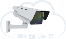
CamStreamer Clouds allows you to use special features such as Remote Access for management connected Axis cameras, TimeLapse, or Cloud Recordings. It also allows you to use our CamStreamer streaming apps as a service on a monthly payment basis. CamStreamer Cloud is not for managing all your perpetual licenses. Still, if you already have perpetual licenses, you can access them via cloud Remote Access if this service is active on specific cameras.
Learn more about CamStreamer Cloud Solutions